
SPI
SPI Overview
SPI, abbreviation of Serial Peripheral Interface, is defined by Motorola on its processors of MC68HCXX Series first. The SPI interface is mainly applicable to EEPROM, FLASH, real-time clock, AD converter, digital signal processor and digital signal decoder. SPI, as a high-speed, full-duplex, synchronous communication bus, imports the principle of "master" and "Slave" devices. In any explicit SPI communication, there will be a master device and one or more slave devices. The master device is responsible for starting and ending communication sessions. The cellular module is the master device in SPI communication by default, while the external device is the slave device. If you need the cellular module to be the slave device, please contact the manufacturer.
A general SPI interface generally contains 4 communication lines:
- SCK: Its main function is to transmit clock signals from the master device to the slave device and control the timing and rate of data exchange.
- SS/CS: Chip select between the slave device and the master device, as a result, the selected slave device can be accessed by the master device;
- SDO/MOSI: Also called Tx-Channel on the master device. As a data output port, it is mainly used for sending data in SPI device;
- SDI/MISO: Also called Rx-Channel on the master device, As a data input port, it is mainly used for receiving data in SPI device;
The SPI communication is full-duplex, which means the data can be transmitted in both directions simultaneously. For SPI, this is implemented via the MOSI (Master Out, Slave In) and MISO (Master In, Slave Out).
In SPI, it owns a total of 4 working modes, which are determined by different configurations of clock polarity (CPOL) and phase (CPHA), see following table:
| SPI Mode | CPOL | CPHA |
|---|---|---|
| 0[00] | 0 | 0 |
| 1[01] | 0 | 1 |
| 2[10] | 1 | 0 |
| 3[11] | 1 | 1 |
SPI Applications on different platforms
The BC25PA platform only supports SPI working modes 0 and 3, and other platforms support all working modes.
QuecPython SPI API Illustration
Build function
class machine.SPI(port, mode, clk)
Parameters:
- port - channel selection, Type: int. Before selecting a channel, It is recommended to check the WIKI and approach the channel corresponding to the SPI pin used.
- mode - SPI working mode. When selecting the working mode, please check the external SPI communication chip data manual to see which modes will be supported by chip. For example, MCP2515 only supports two modes: 0 and 3. In such situation, only mode 0 or mode 3 can be selected.
- clk - clock frequency. Different platforms support different maximum and minimum clock frequencies. The maximum and minimum clock frequencies will be varied in accordance with different platforms. For example, the ASR platform supports a maximum clock frequency of 52MHz and a minimum of 812kHz. When selecting the clock frequency, it is suggested to select a higher frequency as much as possible to increase the communication rate in condition that it is lower than the maximum supported clock frequency of the external SPI communication chip.
SPI Read interface
SPI.read(recv_data, datalen)
This method is used to read the data.
Parameters:
- recv_data - Read data array. Type: bytearray. After the data is read successfully, the corresponding data will be written into recv_data.
- datalen - Read data length. Type: int. Please note that datalen cannot be larger than the actual length of recv_data.
Return Value:
Success: 0, Failure: -1
SPI Write interface
SPI.write(write_data, datalen)
This method is used to write the data.
Parameters:
- write_data - data that needs to be written, Type: bytes.
- datalen - the length of the written data. Type: int. Please note that datalen cannot be larger than the actual length of data.
SPI Read & Write interface
SPI.write_read(recv_data, data, datalen)
This method is used to write and read data simultaneously. SPI communication in essence is the data exchange between the master device and the slave device. In each clock cycle, the SPI device will send and receive the data with one bit (regardless of the master device or the slave device), which means the data with one bit is exchanged. Therefore, the SPI device will write data when reading data and vice versa. The above read interface and write interface in SPI just ignore the other party's data in stage of usage.
Parameters:
- recv_data - read data array, Type: bytearray.
- data - The data has been sent, Type: bytes.
- datalen - the length of data has been written, Type: int. Please note that datalen cannot be larger than the actual length of data.
SPI Bus Applications
Interact with MCU
When interacting with the MCU, the cellular module acts as the Master device and the MCU acts as the Slave device. Before that, relevant corresponding protocol which defines the connotation of data read and written by cellular module clearly shall be provided by MCU side. At this time, the MCU side is similar to an ordinary SPI peripheral and needs to provide the reading and writing meaning of the register. When the cellular module writes a value into the register, the MCU can obtain the commands of the cellular module; meanwhile, the MCU can independently update the register (analog) value and wait for the cellular module to read and obtain the MCU data.
Examples are as follows::
1.Virtual register table in MCU
| Register number | Read and write properties | Register data length | Connotation |
|---|---|---|---|
| 0 | W | 1 | GPIO1 /MCU GPIO1 level status. When writing 1, MCU pulls GPIO1 in high level. |
| 1 | R | 1 | Whether the initialization in MCU is done |
- The protocol is defined as follows:
The cellular module sends: 0x7F (packet header) + 8-bit control segment (0: read command, 1: write command) + 8-bit register number + 8-bit data length + N bytes of data (That will be empty when reading the command)
When the MCU receives the cellular module data and determines that the data is legal, the MCU will reply:
0x7E (packet header) + 8-bit register number + 8-bit data length + N bytes of data (That will be empty when reading the command)
- Example:
Cellular module -> MCU: 0x7F 0x00 0x01 0x01 (read 1 data from register)
MCU -> Cellular module: 0x7E 0x01 0x01 0x01 (MCU initialization is complete)
SPI LCD Display
It owns two methods to connect SPI LCD based on cellular modules, one is a dedicated LCD SPI interface and the other is general SPI.
The connection lines between the cellular module and the LCD display are shown in the figure below:
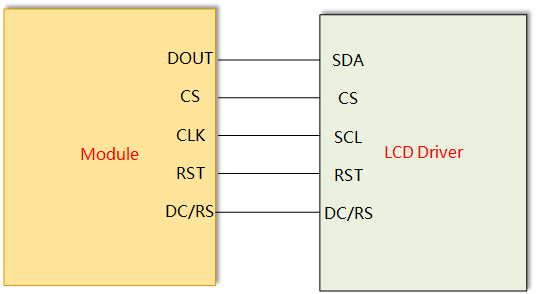
- The DOUT pin is used for serial data transmission. It is a bilateral data communication line between the LCD display and external device such as a controller or micro-controller.
- The SCL/CLK pin is used for clock synchronization during serial data transmission. It provides the clock signal for data transmission for sake of ensuring the proper data synchronization and transmission.
- The RS/DC pin is used to indicate the type of data sent to the LCD, i.e. data or command. When the RS/DC pin is low, it means a command is sent; when the RS pin is high, it means data is sent.
- The RST pin is used to reset the LCD display to its initial state. When the RST pin receives a reset signal, the display will re-initialize and clear the previous status and data.
- The CS pin is used to select or activate the LCD chip. When the CS pin is low, which indicates that the chip is aimed at communication or operation.
When the LCD SPI pin connects to the LCD, the RS, RST and CS pins can only select as specified in the hardware manual. For example, in EC600U series, the CS pin, RST pin and RS pin will be 65, 64 and 63 respectively. See LCD SPI interface initialization as follows:
lcd.lcd_init(lcd_init_data, lcd_width, lcd_hight, lcd_clk, data_line, line_num, lcd_type, lcd_invalid, lcd_display_on, lcd_display_off, lcd_set_brightness)
When the general SPI pin connects to the LCD, the RS, RST and CS pins can be selected according to actual demand, but the pin number needs to be specified in initialization. See following contents in detail:
lcd.lcd_init(lcd_init_data, lcd_width, lcd_hight, lcd_clk, data_line, line_num, lcd_type, lcd_invalid, lcd_display_on, lcd_display_off, lcd_set_brightness, lcd_interface, spi_port, spi_mode, cs_pin, dc_pin, rst_pin)
Compared with LCD SPI pins, SPI mode, SPI port, CS, DC, and RST pins are added to the initialization parameters.
For specific examples, please refer to codes in WIKI-LCD.
MCP2515 CAN Controller
Most CAN controllers in market use SPI bus communication, among which, the MCP2515 is the most widely used. Therefore, in this chapter, it will introduce how to use the Quecpython SPI module to communicate with MCP2515.
The MCP2515 connection diagram is as follows:
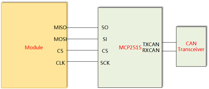
The following contents display the codes for the SPI interface used in the MCP2515 driver.
# Initialize SPI. SPI port: 0. Working mode: 0. Band-rate:6.5MHz (EC800M module)
self.spi = SPI(0, 0, 3)

# Read a single register value. INSTRUCTION.INSTRUCTION_READ: 0x03 (read command)
# Parameters: reg: register number
def readRegister(self, reg):
    write_buf = bytearray([INSTRUCTION.INSTRUCTION_READ, reg, 0x00])
    read_buf = bytearray(len(write_buf))
    ret = self.spi.write_read(read_buf, write_buf, len(write_buf))
    if(ret != 0):
        print("readRegister ret = ",ret)
    return read_buf[2]

# Read multiple register values continuously
# Parameters:reg: initial register number. n: number of registers to be read continuously
def readRegisters(self, reg, n):
    write_buf = bytearray(2+n)
    write_buf[0] = INSTRUCTION.INSTRUCTION_READ
    write_buf[1] = reg
    read_buf = bytearray(len(write_buf))
    ret = self.spi.write_read(read_buf, write_buf, len(write_buf))
    if(ret != 0):
        print("readRegisters ret = ",ret)
    return read_buf[2:]

# Write a single register value INSTRUCTION.INSTRUCTION_WRITE: 0x02 (write command)
# # Parameters: reg: register number, value: the value written into register
def setRegister(self, reg, value):
    write_buf = bytearray([INSTRUCTION.INSTRUCTION_WRITE, reg, value])
    ret = self.spi.write(write_buf, len(write_buf))
    if(ret != 0):
        print("setRegister ret = ",ret)

# Write multiple register values continuously. INSTRUCTION.INSTRUCTION_WRITE:0x02 (write command)
# Parameters: reg: register number, values: the values to be written into registers (bytearray)
def setRegisters(self, reg, values):
    write_buf = bytearray([INSTRUCTION.INSTRUCTION_WRITE, reg]) + values
    ret = self.spi.write(write_buf, len(write_buf))
    if(ret != 0):
        print("setRegisters ret = ",ret)
SPI Bus FAQ and Error Investigation
1.Hardware connection problem: The SPI interface requires four lines (MISO, MOSI, SCLK and CS) for connection. If these lines are not connected correctly, it may cause communication failure.
2.Power and GND issues: If the power and the GND of the SPI device are not connected correctly, it may also cause failed comminication.
3.SPI mode error: SPI has four modes, which are determined by clock polarity and phase. If the SPI modes of the master and slave devices do not match, the communication error may occur.
4.Clock frequency is unduly high: If the clock frequency of SPI is set unduly high, which exceeds the capability of the device, data transmission errors will appear.
5.Mismatch of data bits: The SPI data is usually 8 or 16 bits. If the number of data bits sent and received do not match, data errors may occur as well.
6.Chip selection line control error: In a system with multiple slave devices, if the chip select line is not controlled correctly, communication chaos may occur.
7.Level mismatch problem: If the levels of the master device and the slave device (i.e., 3.3V and 5V) do not match, it may cause communication problems or device damage.
8.Device compatibility issues: Since there is no official standard for SPI, the implementation of different devices may be varied, which may cause compatibility issues between devices.
9.Line Noise and Interference: If the SPI line is too long or there exists high-frequency noise in the environment, it may affect the SPI signal quality and cause communication errors.