
Hardware Introduction
This section demonstrates how to debug an accelerometer sensor based on LTE OPEN-EVB_V1.1, EC600U TE-A EVB, and LIS2DH12TR sensor.
The LIS2DH12TR sensor is a high-performance 3-axis linear accelerometer sensor with digital I2C and SPI serial interface standard output. The sensor has ultra-low power consumption mode, which can achieve features such as advanced power saving, smart, sleep wake-up and sleep recovery. The LIS2DH12TR has a dynamic user-selectable full-scale range of ±2 g/±4 g/±8 g/±16 g and can measure acceleration with output data rates ranging from 1 Hz to 5 kHz. The device can be configured to generate interrupt signals through independent inertial wake-up/free-fall events and the device's position. The threshold and timing of the interrupt generator can be dynamically set by the end user.
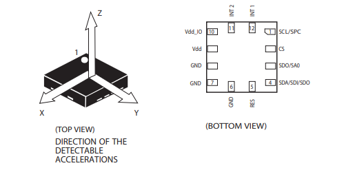
Package Specification
LIS2DH12TR sensor package specifications:
Hardware Connection
Pin function introduction:
| Pin Number | Pin Name | Description |
|---|---|---|
| 1 | SCL SPC |
I2C/SPI clock pin. |
| 2 | CS | SPI enablement pin, used to control the chip communication mode. 1: I2C communication; 2: SPI communication. |
| 3 | SDO SA0 |
Data output pin in SPI mode; Device slave address selection pin in I2C mode. 1: 0x19; 0: 0x18. |
| 4 | SDA SDI SDO |
Data pin in I2C mode; Data input/output pin in SPI mode; |
| 5 | RES | Ground. |
| 6 | GND | Ground. |
| 7 | GND | Ground. |
| 8 | GND | Ground. |
| 9 | Vdd | Power supply. |
| 10 | Vdd_IO | IO reference level pin. |
| 11 | INT2 | Interrupt pin 2. |
| 12 | INT1 | Interrupt pin 1. |
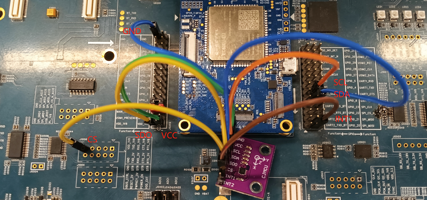
In this section, we use the I2C interface for communication, and the power supply voltage is 1.8 V. The specific wiring is as follows: connect VCC to pin 2 of J0202, GND to pin 30 of J0202, SCL to pin 17 of J0201, SDA to pin 14 of J0201, SDO/SA0 to pin 1 of J0202, CS to pin 9 of J1006, and INT1 to pin 2 of J0201. The wiring diagram between the LIS2DH12 sensor and the EVB is as follows:
The SDO/SA0 pin is at a high level, so it can be confirmed that the slave address of the accelerometer sensor is 0x19.