
GPIO- General-Purpose Input/Output
Basic Knowledge
It will benefit us a lot by learning about basic knowledge on GPIO.
Framework
The GPIO (Abbreviation of General-purpose input/out), a kind of input/output interface for general data, communicates with external electrical components or devices, which can be deployed in micro-processor, micro-controller and other embedded systems.
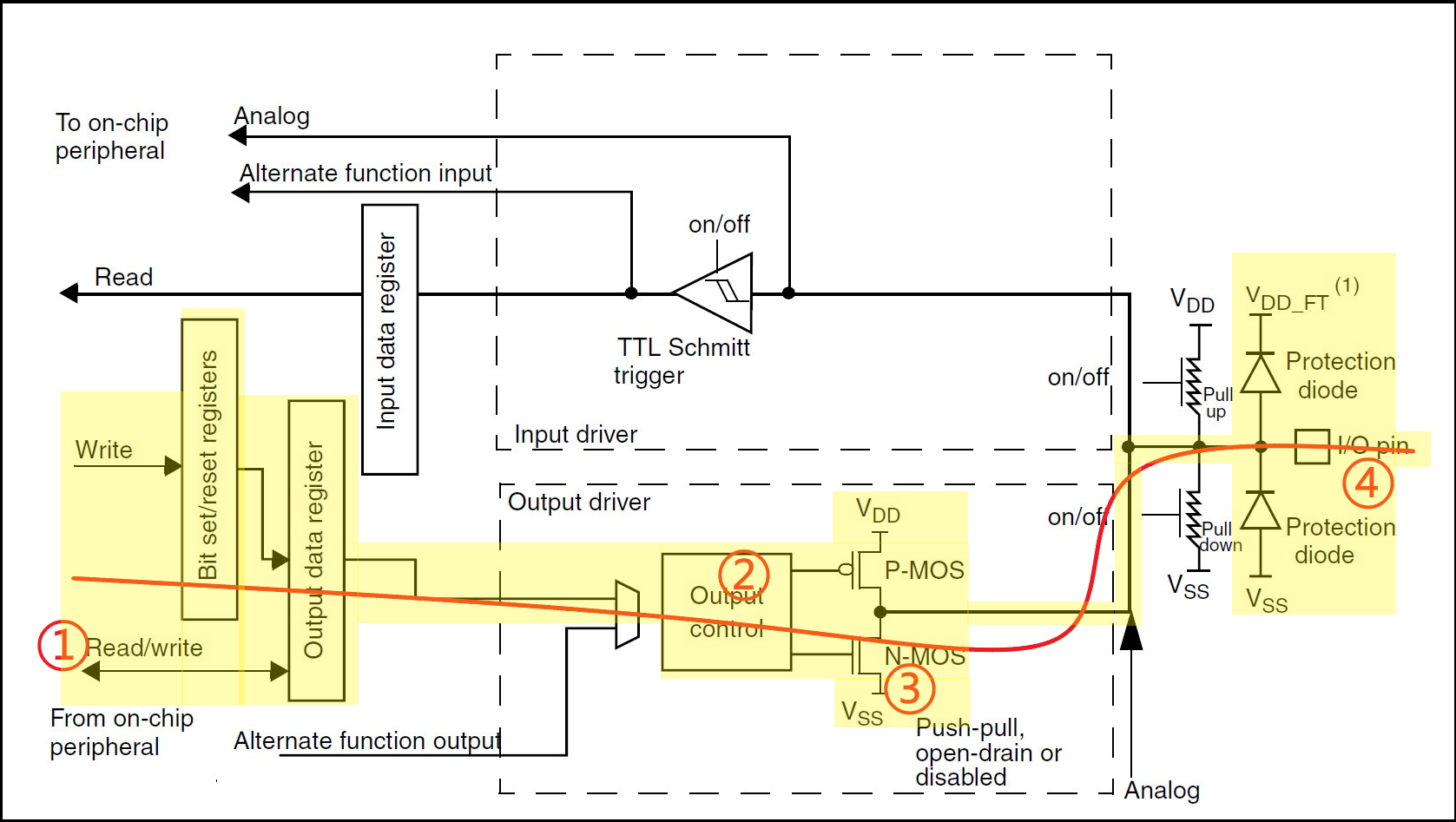
See basic diagram as below:
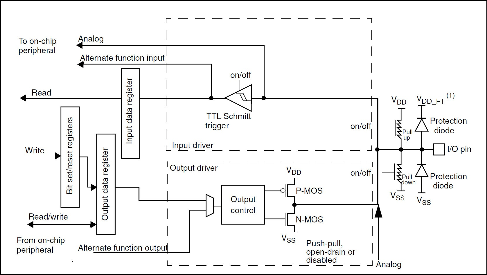
I/O pin: The actual HW interface in micro-processor or micro-controller that connects to external device. Each GPIO pin can be programmed as input or output mode.
Protection diode: One special diode that protects the I/O pin in micro-controller or micro-processor from influence caused by voltage kick-out or ESD.
Pull-up/down resistor: It sets the status of GPIO pin in IDLE or in condition of invisible input signal. The Pull-up resistor will connect the GPIO pin to the positive to set it as the default high-level status. While the Pull-down resistor will connect the GPIO pin to the GND to set it as the default low-level status. Both of them will be controlled by register configured by SW.
P-MOS and N-MOS: The circuit with P-MOS and N-MOS will facilitate GPIO with "Push-pull" and "Open-drain" modes.
TTL Schmitt trigger: Process noise or unstable input data. It will eliminate the noise of data signal based on highest threshold and lowest threshold to provide more accurate digital signal.
Output driver: Control the voltage and current of GPIO pin in output mode
Input receiver: Process input signal from GPIO pin. In most cases, one TTL Schmitt trigger will be embedded to eliminate the noise of digital signal.
Working mode
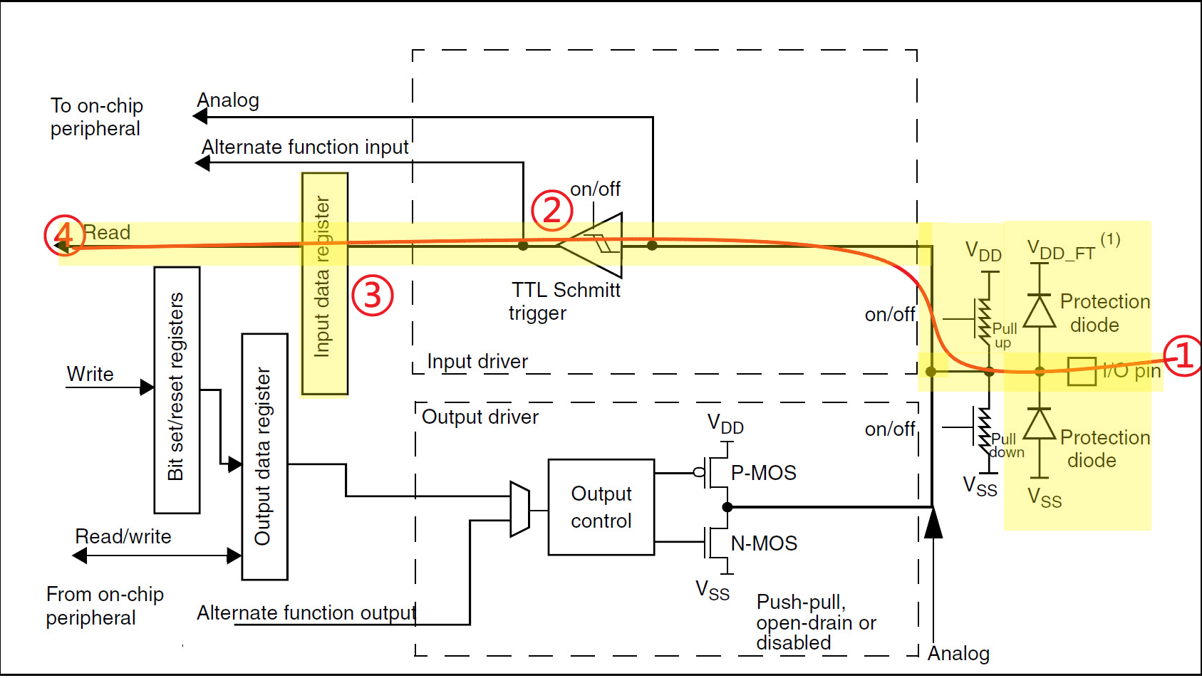
Floating input
Called as Hi-Z, it means the GPIO pin will be floating without being pulled to any logic level. In this status, the GPIO pin can pick up voltage noise easily and read random value. Therefore, please avoid it unless given reason.

The contents highlighted by yellow background illustrates the data transmission channel. The external level signal will enter the internal chip via the I/O with number ①; After that, reformed by Schmitt trigger with number ②, the signal will arrive at "Input data register" with number ③ and ends at the other terminal (Number ④) of "Input data register". Thus, it is available to read the level change of I/O via internal data bus as you wish.
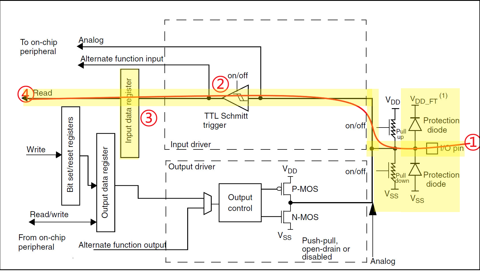
Pull-up input
The pull-up resistor is linked between GPIO pin and VDD. Therefore, under the circumstance that the GPIO pin is not driven by device actively, it will be pulled up to logic high level. In condition that the default status of GPIO pin is high level, please configure it as pull-up mode.
Compared with aforementioned floating input, one pull-up resistor ranged 30KΩ~50KΩ is connected in data channel. In condition that there is no signal input in I/O, the level in input terminal can maintain high (The VDD goes through pull-up resistor). In addition, when the level input in I/O is low, the level in input terminal will be low as well.
Pull-down input
The pull-down resistor is linked between GPIO pin and VSS. Therefore, under the circumstance that the GPIO pin is not driven by device actively, it will be pulled down to logic low level. In condition that the default status of GPIO pin is low level, please configure it as pull-down mode.
In terms of input pull-down mode, one pull-down resistor ranged 30KΩ~50KΩ is linked in data channel.
Analog input
There is neither pull-up resistor nor pull-down resistor and the signal will enter analog input channel without going through Schmitt trigger. Normally, it will be used in ADC data sampling.
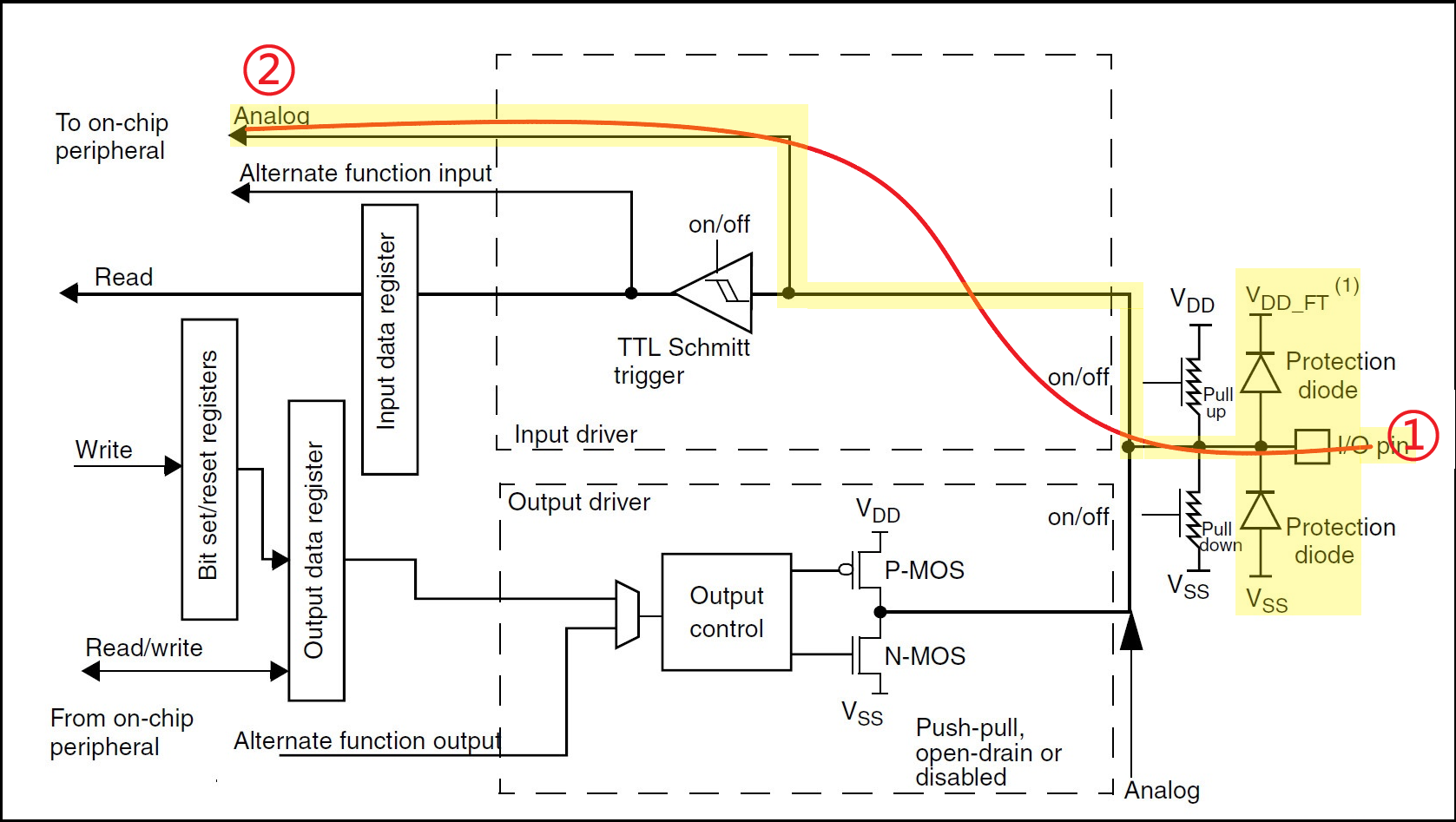
Open-Drain output
In Open-Drain output mode, the GPIO pin will pull down voltage actively via connecting to GND instead of pulling up. If it is needed to pull up voltage, one extra pull-up resistor shall be connected to power supply. It will be applied in I2C communication normally, among which, multiple devices can share one data cable synchronously.
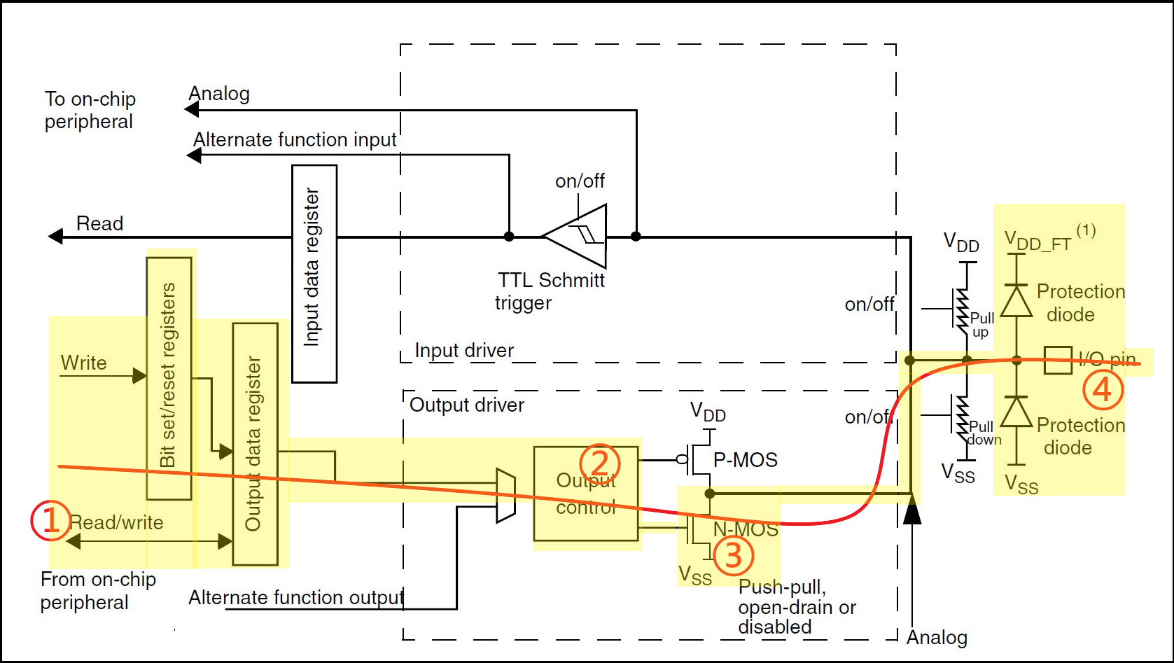
In condition that the CPU writes into data via "Bit set/reset registers" or "Output data register" with number ①, this data bit will be transferred to I/O with number ④ via the "output control circuit“ with number ②. If the logic "1" is written by CPU, the N-MOS with number ③ will be off and the level in I/O is determined by external pull-up resistor. While the logic "0" is written, the N-MOS with number ③ will be on and the level in I/O will be pulled down to zero correspondingly.
As above figure shows, the Schmitt trigger is switched on, which means the CPU can monitor the I/O on other side of "Input data register". Based on this characteristic, it is also available to implement the virtual bilateral communication in I/O. Assuming that the CPU outputs logic "1", the level in I/O will be determined by external circuit completely since the N-MOS with Number ③ is off. Therefore, the CPU is capable to read the external circuit signal in "Input data register" instead of logic "1" outputted by itself.
Push-pull output
In Push-Pull output mode, the GPIO pin will drive high level or low level actively. That means the GPIO can not only push the voltage to high level but also pull voltage to low level. This mode can provide powerful driver, which is suitable for load such as LED and motor.
The most prominent characteristic of push-pull output lies in that it can output high level and low level truly. Moreover, it is equipped with driver in both levels.
Interrupt Framework

Interrupt Mask Register: This register will mask or disable dedicated interrupt for sake of preventing it from triggering interrupt service routine (Abbreviated as ISR hereinafter). When the certain bit is set as 1, the corresponding interrupt will be masked.
Pending Request Register: This register will store the pending interrupt request. Once the value in corresponding bit is 1, which means the relevant interrupt is pending.
Software Interrupt Event Register: This register allows software to generate interrupt. The interrupt service routine (ISR) related to dedicated interrupt will be triggered by writing into this register.
Rising Trigger Selection Register: This register will trigger interrupt in rising edge of signal.
Falling Trigger Selection Register: This register will trigger interrupt in falling edge of signal.
Edge Detector Circuit: This is HW circuit, which will trigger interrupt by detecting the change in rising edge or falling edge.
Timing Mask Register: This register will mask the interrupt generated in specific time. Normally, it will eliminate the interrupt triggered in a error way.
Pulse Generator: It will generate a series of pulse in HW, which will trigger timing or synchronized event, including interrupt.
NVIC (Nested Vectored Interrupt Controller): As a part of ARM Cortex-M, it will manage interrupts, especially the nested and interrupt vector, that is the pointer points at interrupt service routine.
Function Multiplexing
In embedded systems, including plenty of micro-controllers and micro-processors, some dedicated physical pins can be configured as different functions, that is called Pin Multiplexing. Then, how to understand it? The key point is to learn that some pins can be converted among different HW components, resulting in huger flexibility in stage of HW design. The purpose of pin multiplexing is to reduce space and cost since the quantity of physical pins will be decreased.
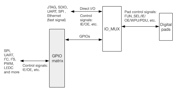
The physical pins of an embedded chip may be designed to switch among several functions
- General data Input/output as GPIO;
- As a part of SPI interface, it will communicate with other SPI devices;
- As a part of UART interface, it will used in serial communication;
- Or it is endowed with other specialized functions such as ADC input or PWM output.
In stage of embedded system design, it is available to configure these pins according to HW and SW demands. In addition, it is also allowed by some embedded platforms to convert these pins dynamically when operating, providing much flexibility.
Absolutely, each coin has two sides, the pin multiplexing also owns limitation. I.e. one pin is not allowed to execute two or dmore functions at the same time. Therefore, please take it into consideration during the period of system design. Moreover, the pin multiplexing management will induce the system complexity and more SWs are demanded to configure and use these pins properly.
Debounce
Button debounce is common issue when processing mechanical button input in corresponding system. Due to its characteristic, the touch point will be opened or closed for several times in a rapid way when pressing or releasing button, resulting in multiple level change in ultra-short time, that is called "bounce". The system may mistake the button for being pressed or released more than once if the bounce is not eliminated. Therefore, please take measures to eliminate or decrease it at least.
Normally, it is divided into two classes- HW debounce and SW debounce.
HW debounce
The purpose of HW debounce is to process the bounce caused by mechanical button and acquire one stable and undisturbed level signal. See following common methods.
RC filter:
Component
- Resistor(R): Connect to one end of button
- Capacitor(C): Connect with the other end of button to GND
Characteristic
- LPF (low-pass filter): Due to its structure, the RC filter will allow the low frequency signal to pass and filter high frequency signal.
Operation
- When the button is pressed or released, the capacitor will start charging or discharging. Therefore, for rapid voltage changes (such as those due to contact bounce), the RC filter smooths these changes, thereby preventing mis-judgements.
- The strength of this smoothing effect is determined by the RC time constant (τ = R×C). This time constant represents the time it takes the capacitor to charge to 63.2% of its initial voltage.
Common parameters
- Resistor(R): 1kΩ ~10kΩ
- Capacitor(C): 0.1µF~10µF
Advantage:
- Simplicity: Only two basic components are needed
- Economy: Both resistor and capacitor are low-cost
- Effectiveness: In terms of majority of common applications, the debounce capability is sufficient.
Disadvantage
- Delay: The ultra huge RC time constant will cause unnecessary delay in button response.
- Environment sensitivity: The variation in temperature and humidity may influence the capacitor value and debounce effect further.
- Not all applications can be applied: For quick-response application, the RC filter will not be the optimum selection.
If the RC filter is taken in HW debounce solution, the suitable resistor and capacitor values are important since it will filter bounce effectively without inducing excessive response delay at the same time. Therefore, in design stage, it is necessary to test different combinations of R and C to achieve optimum debounce effect.
Schmitt Trigger:
Component
- Schmitt trigger: In essential, it is a power comparator with dual threshold. Due to its characteristic, it can not only be one independent component but also a part of micro-controller.
Characteristic
- Dual threshold: The main characteristic of Schmitt trigger lies in that it owns two thresholds- Vt+ & Vt-.
Operation
- Once the input voltage rises and surpasses the Vt+, the output will switch to high status.
- Once the input falls and is lower than Vt-, the output will switch to low status.
- This characteristic can guarantee that the output status will not change if any minor change in input voltage so as to filter bounce effectively.
Common parameter
- Vt+ & Vt-: The gap between two thresholds is called as hysteresis or dead zone.
Advantage
- Perfect debounce: Owing to dual threshold characteristic. the Schmitt trigger is endowed with powerful tolerance in input noise and bounce.
- Explicit output: The output will be either low or high level, which will not fluctuate between them.
- Widespread application: The input of GPIO in multiple micro-controllers are embedded with optional Schmitt trigger.
Disadvantage
- Possible delay: In some cases, if the change in input signal is slow, the trigger will cause minor delay.
- Inadequate fast signal: In terms of signal with high frequency, the Schmitt trigger will not be the optimum since it will lead to signal distortion
- Cost: Although many micro-controllers are embedded with Schmitt trigger. If the external trigger is needed, the cost will increase as well.
Notes
- As for selected debounce method and component value, please consider the bounce frequency and duration.
- If RC filter is deployed, please confirm the RC time constant can eliminate bounce without unduly delaying the button response.
- If it works in environment with noise, please consider other elements such as external EMI (Electromagnetic Interference)
- The test plays a vital role. After the design is complete, the system should be tested enough to ensure that the debounce circuit will work properly under all expected conditions.
Shunt capacitor
Component
- Capacitor (C): Connect with key directly. Normally, it will connect with one terminal of button and the GND.
Characteristic
- Delayed charging/discharging: Owing to its characteristic, the capacitor should take time in charging and discharging
Operation
- Under the circumstance that the button is not pressed yet, the capacitor will in discharging status.
- Once the button is pressed, it will spend certain time in charging till the capacitor is full, which will do a favor in filtering the short bounce that may occur.
- Similarly, when the button is released, the capacitor will discharge in due time so as to eliminate possible bounce.
Common parameters
- Capacitor (C): 1nF ~10µF. The specific value is determined by dedicated demand and the frequency of key bounce.
Advantage:
- Simplicity: Only one capacitor is needed and the connection is simple as well
- Low cost: The capacitor is cheap and easy to acquire.
- Apparent effect: It will debounce heavily in terms of most of common button bounces.
Disadvantage:
- Possible delay: Ultra-huge capacitor will lead to obvious delay in key response.
- Environment sensitivity: The variation in temperature and humidity may influence the capacitor value and debounce effect further.
- Power noise: If the power noise is generated by other components in system, this shunt capacitor may magnify the noise.
- Not all applications can be applied: For quick-response application, this method will not be the optimum.
RS trigger
Component
- RS trigger: Normally, the basic bistable circuit is made by two NAND gates or NOR gates.
- Two Inputs: R (Reset) & S (Set)。
- Two outputs: Q & ~Q (Inversion of Q)。
Characteristic
- Bistable: The RS trigger always owns two stable output statuses
Operation
- In condition that the input in S is 1 and the input of R is 0. the output of Q will be 1 while the ~Q will be 0.
- In condition that the input in R is 1 and the input of S is 0. the output of Q will be 0 while the ~Q will be 1.
- Under the circumstance that both inputs are 0, the RS trigger will maintain current status
- Under the circumstance that both inputs are 1, this status is not allowed and uncertain output will be triggered probably.
In order to eliminate button bounce, the RS trigger can be configured as the situation that only when the button is truly pressed or released can the status be changed. Any momentary bounce related to button will not change the output of RS trigger, leading to effective debounce.
Common parameter
- Input logic level:
- For RS trigger of NAND, the common logic level is 1;
- For RS trigger of NOR, the common logic level is 0.
Advantage:
- High effective debounce: The RS trigger provides stable output for button no matter how noisy the input.
- Explicit output status: There will be high or low output in any given time.
- Low cost: The RS trigger can be built by basic logic gate.
Disadvantage:
- Complexity: Compared with simple shunt capacitor or Schmitt trigger, more components and more complex traces are needed.
- Impermissible status: There exists one impermissible status in RS trigger, please avoid in stage of design.
- Power supply demand: Appropriate power shall be provided for RS trigger
Proprietary debouncer
There are some proprietary debouncers such as MAX6816, MAX6817 and MAX6818 in market. The filter and Schmitt trigger involved in these ICs can be valid to connect to button and provide stable data output.
Notes
- As for selected debounce method and component value, please consider the bounce frequency and duration.
- If RC filter is deployed, please confirm the RC time constant can eliminate bounce without unduly delaying the key response.
- If it works in environment with noise, please consider other elements such as external EMI (Electromagnetic Interference)
- The test plays a vital role. After the design is complete, the system should be tested enough to ensure that the debounce circuit will work properly under all expected conditions.
SW debounce
This method will eliminate button bounce via algorithm and logic in SW. Compared with former method, it provides more flexibility in terms of different applications and conditions as well as burden increased.
See common embedded SW debounce methods:
Delay
Operation
Once the button status changes (I.e. Change from never-pressed status into pressed status), the program will wait one predetermined delay time instead of responding this change immediately. After this delay is over, the program will detect button status again. If the button status maintains, this operation will be considered as valid and the program will respond it. Otherwise, it will be taken as error or bounce, resulting in no response.
Advantage:
- Simple implementation: The delay will be simplest and targeted SW debounce method by adding one delay function after the button status is changed.
- No extra resource is needed: Compared with other methods such as counter or FSM, neither extra storage nor counting resource are needed in this method.
Disadvantage:
- Response delay: Since it is needed to wait predetermined delay time to confirm the pressed action, the response delay will be caused.
- CPU time consumption: If the busy-waiting is used to implement delay, it will be a failure for CPU to execute any task in this period, which is unacceptable in embedded system with restricted resource.
- Unreliability: If the bounce lasts longer than the predetermined delay time, this method may still produce an error. In addition, if the delay time is set too long, you may miss the rapid continuous button action.
Counter
Operation
When it detects the button status change, the system will not confirm immediately. Instead, one counter will be initiated. In following consecutive tests, if the button status keeps changing, the value in counter will increase corresponding. While the button returns to original status, the counter will be reset instead. Only under the circumstance that the value in counter reaches the pre-determined threshold can the button status change be considered as the true press and responded by system. Thus, the momentary bounce will not reach the threshold of counter and it can't be mistaken for a valid button action.
Advantage
- Perfect reliability: Compared with simple delay debounce, it will filter the momentary bounce more reliably.
- Perfect response: If the button is pressed consecutively, the system will confirm this action in relatively short time to provide faster response.
- Flexibility: It is available to adjust counter threshold via actual need to adapt to different button and bounce characteristic.
Disadvantage
- Resource consumption: It is needed to arrange one counter for each button or one global counter for system, which may consumer extra storage and counting resource.
- Complexity: Compared with simple delay debounce, the debounce by counter will be more complex actually, especially in scenario that needs multiple keys.
- Possible delay: If the predetermined threshold in counter is unduly high, it will cause delayed response in system and bad user feeling.
FSM (finite-state machine)
Operation
It involves defining multiple statuses for button and determines the next status based on current status and input.
Typical FSM will be divided into following several statuses: not pressed, probably pressed, pressed, probably released. The original status is not pressed.
- Once the button is pressed, the FSM will switch to the status of
Probably pressedand initiate timer. - If the timer arrives at defined time and the key is still pressed, the FSM is switched to the
pressedstatus. - Once the button is released, the FSM will switch to the status of
Probably pressedand initiate timer again. - If the timer arrives at specified time and the key is still released, the FSM is switched to the status of
not pressed.
Thus, The state of a button will be confirmed by the system if it remains steadily in a state for longer than the specified time. The short bounce will not cause state change and debounce.
Advantage
- Perfect reliability: The FSM can identify and ignore momentary bounce accurately.
- Flexibility: The FSM structure allows developer to add more statuses and logics such as double-click and long-press.
- Clear logic structure: The FSM provides clear and structured framework for button to facilitate understanding and maintenance.
Disadvantage
- Implementation complexity : Compared with other SW debounce method, the FSM demands more complicated codes and logic.
- Resource utility: The FSM will deploy timer or interrupt and extra storage to save status.
- Possible delay: The FSM structure and timer may lead to delayed button response
Support
See specific supports of QuecPython Series
For details, please refer to the GPIO Multiplexing table of each module.
| Module | Floating input | Pull-up input | Pull-down input | Open-drain output | Pull-push output | Supported quantity |
|---|---|---|---|---|---|---|
| EC200U | √ | √ | √ | × | √ | 47 |
| EC600U | √ | √ | √ | × | √ | 47 |
| EG912U | √ | √ | √ | × | √ | 41 |
| EG915U | √ | √ | √ | × | √ | 41 |
| EC600G | √ | √ | √ | × | √ | 46 |
| EC800G | √ | √ | √ | × | √ | 50 |
| EG912N | √ | √ | √ | × | √ | 40 |
| EG915N | √ | √ | √ | × | √ | 41 |
| EC600N | √ | √ | √ | × | √ | 41 |
| EC600S | √ | √ | √ | × | √ | 41 |
| EC800N | √ | √ | √ | × | √ | 37 |
| EC600M | √ | √ | √ | × | √ | 45 |
| EC800M | √ | √ | √ | × | √ | 44 |
| EG810M | √ | √ | √ | × | √ | 44 |
| EC200A | √ | √ | √ | × | √ | 26 |
| UC200A | √ | √ | √ | × | √ | 26 |
| BG95_XX | √ | √ | √ | × | √ | 21 |
| BG600L | √ | √ | √ | × | √ | 25 |
Annotation:
- √:Support
- ×:Do not support
Function Illustration
It is mainly divided into two types: GPIO and Extlnt.
GPIO
In this chapter, it will introduce how to use QuecPython GPIO and relevant notes.
For specific API on QuecPython GPIO, please refer to machine.Pin
Create object
Input/output, pull-up/down and default pin of GPIO can be implemented in this step.
class machine.Pin(GPIOn, [dir], [pull], [value]
For parameter introduction and GPIO pin number & physical mapping, please see machine.Pin.
If the pin is to be available in relevant module, please import it first. Then, you can create one pin as following method.
>>> pin = machine.Pin(1
In this case, the number "1" is the corresponding GPIO number of pin to be visited. Normally, it is hoped to configure this pin as input or output and operate when creating it.
>>> pin = machine.Pin(1, machine.Pin.IN, machine.Pin.PULL_PU)
It is available to take it as input pull-up/down via PULL_PU PULL_PD or PULL_DISABLE .
Read level
Pin.read()
For specific method, please refer to Pin.read.
When the GPIO is configured as input, its inner structure allows itself to detect and reflect the voltage imposed. It is available for you to read this status via querying internal register in micro-controller or Pin.read.
HIGH: The voltage in GPIO is adjacent or equal to that in power supply such as 1.8 V or 3.3 V。
LOW: The voltage in GPIO is adjacent or equal to that in GND.
Applicable scenario
- Button or switch input: By reading the GPIO level, it is available to detect whether the key is pressed or the switch is on/off.
- Receive signal from other digital device: Receive signal sent by devices such as sensor, module or other micro-controllers.
Note
- Pull-up and pull-down resistor: In some cases, the external device won't provide definite status. In order to avoid such "floating" situation, the internal or external pull-up or pull-down resistor can be used.
- Input voltage range: In order to protect micro-controller, please guarantee the input voltage of GPIO shall be within the permissible range.
Output level
Pin.write(value)
For specific method, please refer to Pin.write.
When the GPIO is configured as output mode, it is capable to output high or low level.
- HIGH: The voltage in GPIO is adjacent or equal to that in power supply such as 3.3 V or 5 V。
- LOW: The voltage in GPIO is adjacent or equal to that in GND.
Driver capability
When configured as output, the GPIO is endowed with certain limited driver capability, which means it can provide or sink certain amount of current. If it is demanded to drive relatively huge load, the external circuit such as transistor or relay shall be applied.
Applicable scenario:
- LED Indicator: It is available to switch on/off LED via setting GPIO as high or low.
- Drive relay: It is capable to control motor, light and other housekeeping appliances.
- Communicate with other digital devices: By means of serial communication, SPI and I2C.
Note
- Maximum output current: Each GPIO is restricted with maximum output current. It may ruin micro-controller when trying get excessive current from GPIO pin.
- Output type: Some GPIOs support open-drain/open-source output, which means it can either pull up or pull down instead of driving bilaterally.
Direction
Pin.set_dir(value)
For specific method, please refer to Pin.set_dir.
Direction selection
- IN:
- When the GPIO is configured as input, it will read external device status. I.e. Detect whether the button is pressed.
- OUT:
- When the GPIO is configured as output, it can manipulate external device status. I.e. Switch on/off LED.
Importance of direction
- Electrical protection: If a pin is incorrectly configured as output and attempts to drive a signal that conflicts with another device that is trying to drive the same line, a short circuit or damage may be caused.
- Function: Different inner circuits will be activated by configuration in different directions. E.g. when configured as input, it is possible for GPIO to initiate one Hi-Z circuit to immune other devices connected to itself.
Notes
- Please make sure the GPIO direction has been set properly before connecting to any external device.
- Take overall circuit design into consideration. I.e. if one GPIO is configured as output and connected to one button, please guarantee the GPIO will not be connected to unduly high voltage when it is pressed.
Interrupt
This class is used to configure the I/O pin to trigger an interrupt when an external event occurs
Create object
class machine.ExtInt(GPIOn, mode, pull, callback)
For specific method, please refer to machine.ExtInt.
Types to trigger interrupt
Rising Edge Interrupt
- Applicable Scenario: Detect the moment when the button is pressed or detect the sensor from idle to active status.
Falling Edge Interrupt
- Applicable Scenario: Detect the moment when the button is pressed to released or detect the sensor from active to idle status.
Both Edges Interrupt
- Applicable Scenario: In terms of certain application such as Rotary Encoder for sake of detecting status change, it may demand info of rising edge and falling edge.
Configure pull-up and pull-down resistor internally.
It is allowed for module to configure internal pull-up or pull-down resistor in stage of initializing GPIO.
If the button or switch is connected to GPIO and there exists no external pull-up or pull-down resistor, the internal resistor can ensure that GPIO is in a known state when not driven.
Callback function
When triggering interrupt, it is demanded for module to take charge of dedicated operation or function to be executed, that is called callback function. As a function defined by user, it will be called automatically when specialized interrupt condition is satisfied.
Note: The callback function shall be as short and fast as possible to avoid impending other interrupt or logic of main program for a long time.
Enable/disable
extint.enable()
extint.disable()
For specific method, please refer to Eextint.enable and Extint.disable
Enable
- Definition: It allows GPIO pin to respond in terms of specialized event such as rising edge and falling edge.
- Usage: When the system is ready to process interrupt from specialized GPIO pin, please enable it. I.e. It shall be conducted after the system is initialized or former interrupt is accomplished.
- Operation: There exists dedicated register or command in module to enable specific GPIO interrupt.
Disable:
- Definition: Stop GPIO pin from responding specialized event, that means the interrupt will not generate even if this event occurs.
- Usage: When executing vital codes such as FW upgrade, system calibration or other operation that needs to be immune from interrupt, please disable interrupt. Moreover, it is also used in the preliminary stage of ISR to avoid triggering same interrupt again when processing it.
- Operation: Similar with enabling interrupt, specialized register or command will be embedded in most of micro-controller to disable dedicated GPIO interrupt.
Note
- Time Precision: In certain cases, especially for application with high time precision, it may need to enable or disable interrupt rapidly.
- Global and local: In some systems, it is available to disable all interrupts (disable globally) or specialized interrupt (disable locally).
- Security: After disabling interrupt, it is mandatory to enable it again in appropriate situation. Otherwise, it will cause a failure to respond some vital events in system.
For other method, please refer to wiki -machine.ExtInt in detail.
For other method, please refer to wiki -machine.ExtInt in detail.
Application examples
It mainly introduces applications related to GPIO.
| Example | Description & Application |
|---|---|
| LED controller | Description: When configured as output, it will drive LED to switch on or off. Application: Display system status, notification and warning. |
| Button | Description: When configured as interrupt input, it will respond to external event Application: External device notification, real-time event detection and button debounce. |
| One wire | Description: Dedicated communication protocol. Application: Temperature monitoring, authenticator and device configuration. In this case, the DS18B20 temperature sensor based on One-Wire driver is used. |
| SIF | Description: SIF communication protocol. Application: SIF. Mainly used in E-bike communication. |
The example contains description of individual application scenario, implementation and corresponding protocols.
Notes
Power supply and GND :
- Ensure all devices and main controllers connected by GPIO share the same GND.
- It is not allowed to connect to the GPIO pin to the voltage that beyond specific range; otherwise, it will be damaged.
Current restriction:
- Each GPIO pin is endowed with maximum source current and sink current. Once surpassed, it will ruin pin or entire chip.
- One adequate resistor can restrict the current connected to GPIO pin.
Input mode:
- When the GPIO is configured as input mode, please do not output voltage to it.
- The floating input pin will read random value, therefore, it is suggested to use pull-up or pull-down resistor.
Output mode:
- Do not connect two GPIO output pins directly; otherwise, it will cause short circuit when outputting different level.
- When the pin is set as output mode, try avoid imposing external voltage to it.
Debounce:
- When reading mechanical switch or button via GPIO, it may occur bounce. In this situation, the HW or SW debounce can be applied to solve.
For specific, please refer to Debounce.
Interrupt:
- For application demanding fast-response, the GPIO interrupt should be used instead of polling GPIO status.
- Ensure the ISR as short as possible and avoid impending other interrupt or logic of main program for a long time.
Protection circuit:
- Select adequate components such as TVS diode to protect GPIO pin from being influenced by peak voltage.
- In terms of application processing analog signal, the RC filter should be used.
Peripheral conflict:
- In some micro-controllers, some GPIO pins may be multiplexed with other functions such as PWM, ADC and communication interface. Please take all potential conflicts into consideration when designing.
Thermal design:
- When the massive current goes through GPIO pin, the temperature shall be considered since it will cause over-heat.
Firmware/Software:
- Make acquaintance with current settings before modifying GPIO configuration or status.
- During the period of initiation, please initialize all GPIOs into known status to avoid exceptions.
EMI/RFI:
- The GPIO wire might be the victim of EMI or RFI, as a result, please take some elements into consideration such as adequate layout, grounding and shielding.
Common issues
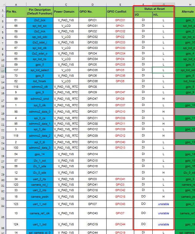
About GPIO Multiplex Table
Displayed by table or document, the GPIO Multiplexing table is used to describe different functions and alternative options of GPIO pins in specialized chip, micro-controller or system. In most of chips and micro-controllers, the GPIO pin is endowed with multiple functions and alternative options. That means each GPIO pin can be configured as various input or output such as data input/output, analog input/output or special peripherals. (I.e. SPI, UART and I2C)
The GPIO multiplexing table of QuecPython illustrates the function and alternative option of each GPIO pin in detail as well as status change in stage of booting. It lists the number, default function and available alternative option of each pin to make it convenient for user to configure and use GPIO pin properly, which is vital in connecting peripherals, driving screen ad controlling communication interface.
The format and contents of specific GPIO multiplexing table will be varied according to different module. Therefore, for given module, please refer to relevant Hardware Design or GPIO multiplexing table for detailed GPIO configuration.
In this case, it will take the QuecPython EC600U GPIO configuration as an example. For other modules, it will be similar.
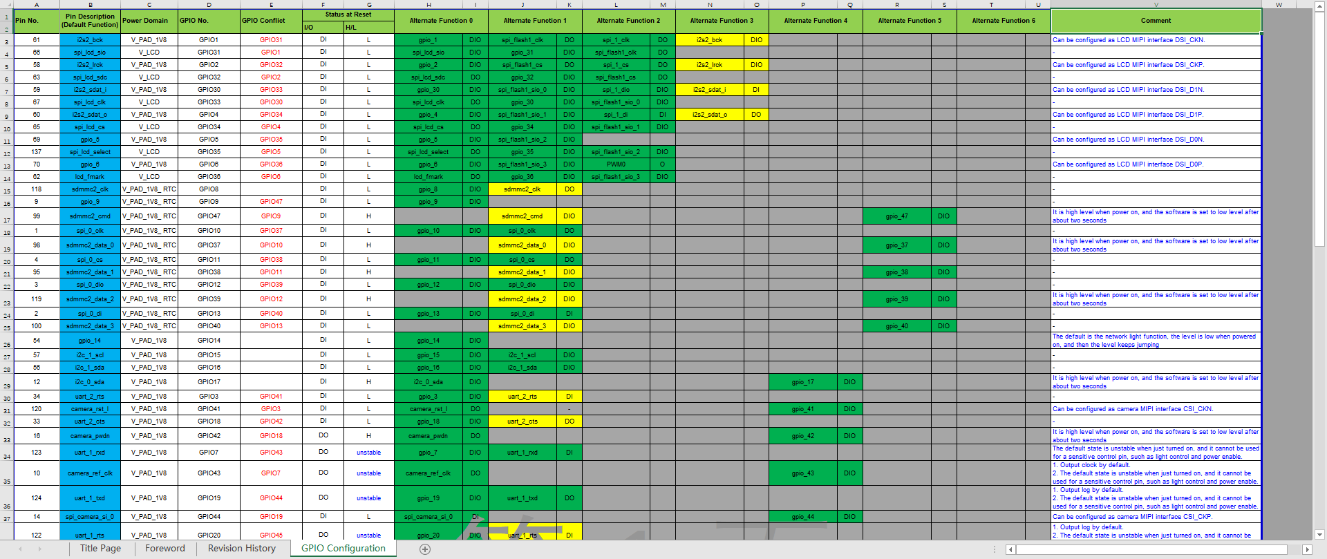
Explanation on each column
| Term | Explanation |
|---|---|
| Pin No. | Module physical pin number |
| Pin Description | Default function of pin |
| Power Domain | Power domain of pin |
| GPIO No. | GPIO number of pin |
| GPIO Conflict | Pin with GPIO multiplexing (It is not allowed to use the pin with conflict GPIO function at the same time) |
| Status at Reset | Status at reset. The level change will be marked in Comment column. |
| Alternate Function | Pin multiplexing function |
| Comment | Notes of pin and level change description in stage of booting |
Status at Reset
The pin at Reset will be varied according to different HW platform and development environment. Normally, when powering up or rebooting system. the initial status of GPIO pin is undefined and is out of control by SW. Therefore, in terms of controlling LED or enabling peripheral switch, the pin with special reset status is needed. Before designing HW circuit, please query relevant documents or references to make acquaintance with pin at Reset in dedicated platform and environment.
The GPIO pin at Reset of individual platform can be acquired via querying GPIO multiplexing table .
Most GPIO pins are stable when powered on, and a small number of GPIO pins are changed by software after powered on. See QuecPython GPIO multiplexing table in detail.
Query pin interrupt function
Query whether there exists interrupt function in pin and corresponding method to trigger interrupt.
Except for BG95 module, all GPIOs support interrupt function.
In terms of BG95 Series, it is also available to get the GPIOs that support interrupt function via querying GPIO multiplexing table.
Wake up interrupt
The GPIOs in EC200U/EC600U/EG912U/EG915U modules support waking up module in sleep mode. While for others, most of which support waking up module. For specific, please query and confirm via GPIO multiplexing table.
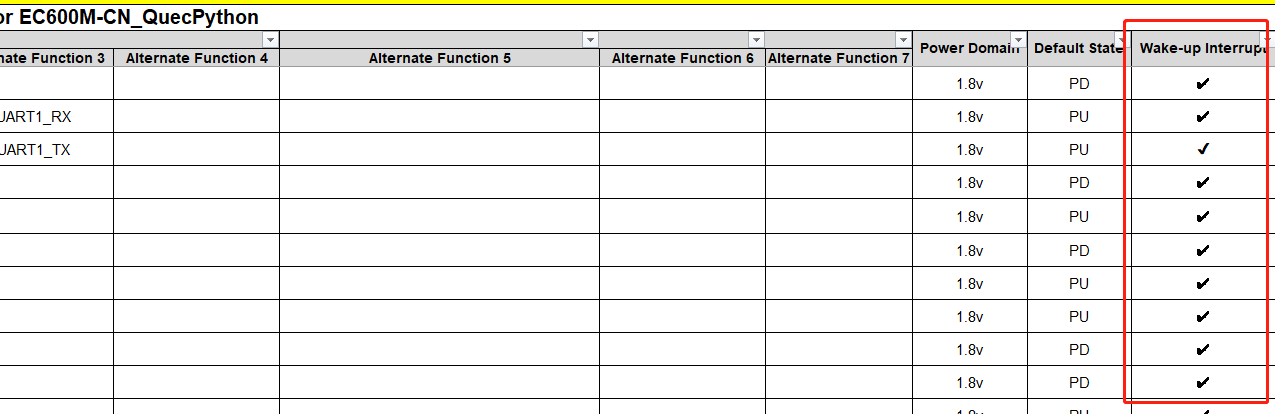
To check whether it supports waking up interrupt, please refer to the GPIO multiplexing table of the corresponding module.
Pin status in sleep mode
The GPIO status remains unchanged after entering sleep mode.