BG95 EVB Introduction
Supported Module List
Feature List
Overview
The QuecPython_BG95_EVB is a compact and portable "pocket-sized" EVB specifically designed for QuecPython.
The main board is equipped with a BG95 series module and a Type-C interface. You can easily develop the EVB with just a USB Type-C cable.
The EVB is also equipped with an expansion board that supports light sensors, UV sensors, VOC sensors, nine-axis sensors, and temperature and humidity sensors.
The EVB is compatible with Raspberry Pi Zero, and the expansion board for Raspberry Pi Zero can be directly used on the QuecPython_BG95_EVB.
Description
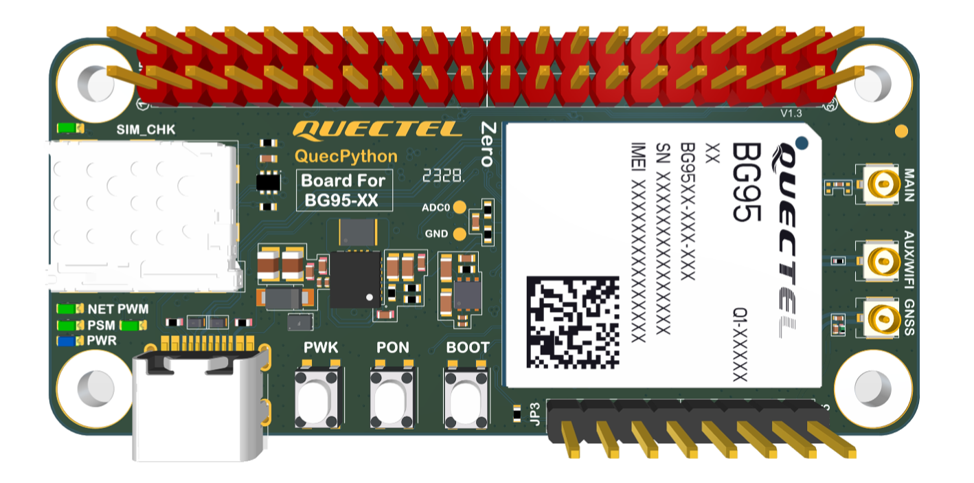
The main components and interface layout of the EVB are shown in the following figure.

Resource Download
EVB Resources
EVB Interface
8 Pin Assignment
| Pin Header | Number | Silkscreen | Pin No. | Function |
|---|---|---|---|---|
| JP6 | 1 | PWK_AUTO | 15 | POWERKEY |
| JP6 | 2 | PWK_AUTO | - | GND |
| JP6 | 3 | VDD_EXT | - | 1.8 V |
| JP6 | 4 | VDD_EXT | 29 | VDD_EXT |
| JP6 | 5 | MODULE_EN | - | 3.6 V |
| JP6 | 6 | MODULE_EN | - | 3.6 V |
| JP6 | 7 | GNSS_EN | - | 3.3 V |
| JP6 | 8 | GNSS_EN | 51 | GNSS_EN |
- 1 & 2: Automatic power-on.
- 3 & 4: connect VDD_EXT to provide power for external circuit. For power consumption measurement, VDD_EXT needs to be disconnected.
- 5 & 6: Turn on the DC-DC converter to provide power to the module.
- 7 & 8: Enable active power supply for GNSS.
40 Pin Assignment
| Pin Header | Number | Name | GPIO Multiplexing | Function | Pin Header | Number | Name | GPIO Multiplexing | Function |
|---|---|---|---|---|---|---|---|---|---|
| JP7 | 1 | 3V3 | - | 3.3 V Output | JP8 | 2 | 5V | - | 5 V Output |
| JP7 | 3 | SDA1 | I2C1_SDA GPIO14 |
I2C1 Data General Purpose Input/Output |
JP8 | 4 | 5V | - | 5 V Output |
| JP7 | 5 | SCL1 | I2C1_SCL GPIO13 |
I2C1 Clock General Purpose Input/Output |
JP8 | 6 | GND | - | Ground |
| JP7 | 7 | P35 | GPIOX UART4_TXD |
General Purpose Input/Output UART4 Send |
JP8 | 8 | TX2 | UART2_TXD | UART2 Send |
| JP7 | 9 | GND | - | Ground | JP8 | 10 | RX2 | UART2_RXD | UART2 Recv |
| JP7 | 11 | P06 | GPIO3 PCM_DIN |
General Purpose Input/Output Digital Audio Input signal |
JP8 | 12 | P37 | GPIOX I2C_SDA |
General Purpose Input/Output I2C Data |
| JP7 | 13 | P05 | GPIO2 PCM_SYNC |
General Purpose Input/Output Digital Audio Sync signal |
JP8 | 14 | GND | - | Ground |
| JP7 | 15 | P04 | GPIO1 PCM_CLK |
General Purpose Input/Output Digital Audio Clock signal |
JP8 | 16 | P86 | GPIO19 | General Purpose Input/Output |
| JP7 | 17 | 3V3 | - | 3.3V Output | JP8 | 18 | P88 | GPIO21 | General Purpose Input/Output |
| JP7 | 19 | MO2 | SPI2_MOSI GPIO8 UART0_TXD |
SPI2 Master Output Slave Input General Purpose Input/Output UART0 Send |
JP8 | 20 | GND | - | Ground |
| JP7 | 21 | MI2 | SPI2_MISO GPIO7 UART0_RXD |
SPI2 Master Input Slave Output General Purpose Input/Output UART0 Recv |
JP8 | 22 | P20 | GPIOX | General Purpose Input/Output |
| JP7 | 23 | CLK2 | SPI2-CLK GPIO5 I2C0_CLK |
SPI2 Clock General Purpose Input/Output I2C0 Clock |
JP8 | 24 | CS2 | SPI2_CS GPIO6 I2C0_SDA |
SPI2 Chip Select General Purpose Input/Output I2C0 Data |
| JP7 | 25 | GND | - | Ground | JP8 | 26 | P38 | GPIOX | General Purpose Input/Output |
| JP7 | 27 | P25 | GPIO9 SPI0_CS |
General Purpose Input/Output SPI0 Chip Select |
JP8 | 28 | P26 | GPIO10 SPI0_CLK |
General Purpose Input/Output SPI0 Clock |
| JP7 | 29 | P34 | GPIOX UART4_RXD |
General Purpose Input/Output UART4 Recv |
JP8 | 30 | GND | - | Ground |
| JP7 | 31 | P87 | GPIO20 | General Purpose Input/Output | JP8 | 32 | PWM | PWM0 GPIO17 |
PWM0 Output General Purpose Input/Output |
| JP7 | 33 | P85 | GPIO18 PWM1 |
General Purpose Input/Output PWM1 Output |
JP8 | 34 | GND | - | Ground |
| JP7 | 35 | P28 | GPIO12 SPI0_MISO UART3_RXD |
General Purpose Input/Output SPI0 Master Input Slave Output UART3 Recv |
JP8 | 36 | P39 | GPIOX | General Purpose Input/Output |
| JP7 | 37 | P07 | GPIO4 PCM_DOUT |
General Purpose Input/Output Digital Audio Output signal |
JP8 | 38 | P27 | GPIO11 SPI0_MOSI UART3_TXD |
General Purpose Input/Output SPI0 Master Output Slave Input UART3 Send |
| JP7 | 39 | GND | Ground | JP8 | 40 | P36 | GPIOX I2C_SCL |
General Purpose Input/Output I2C Clock |
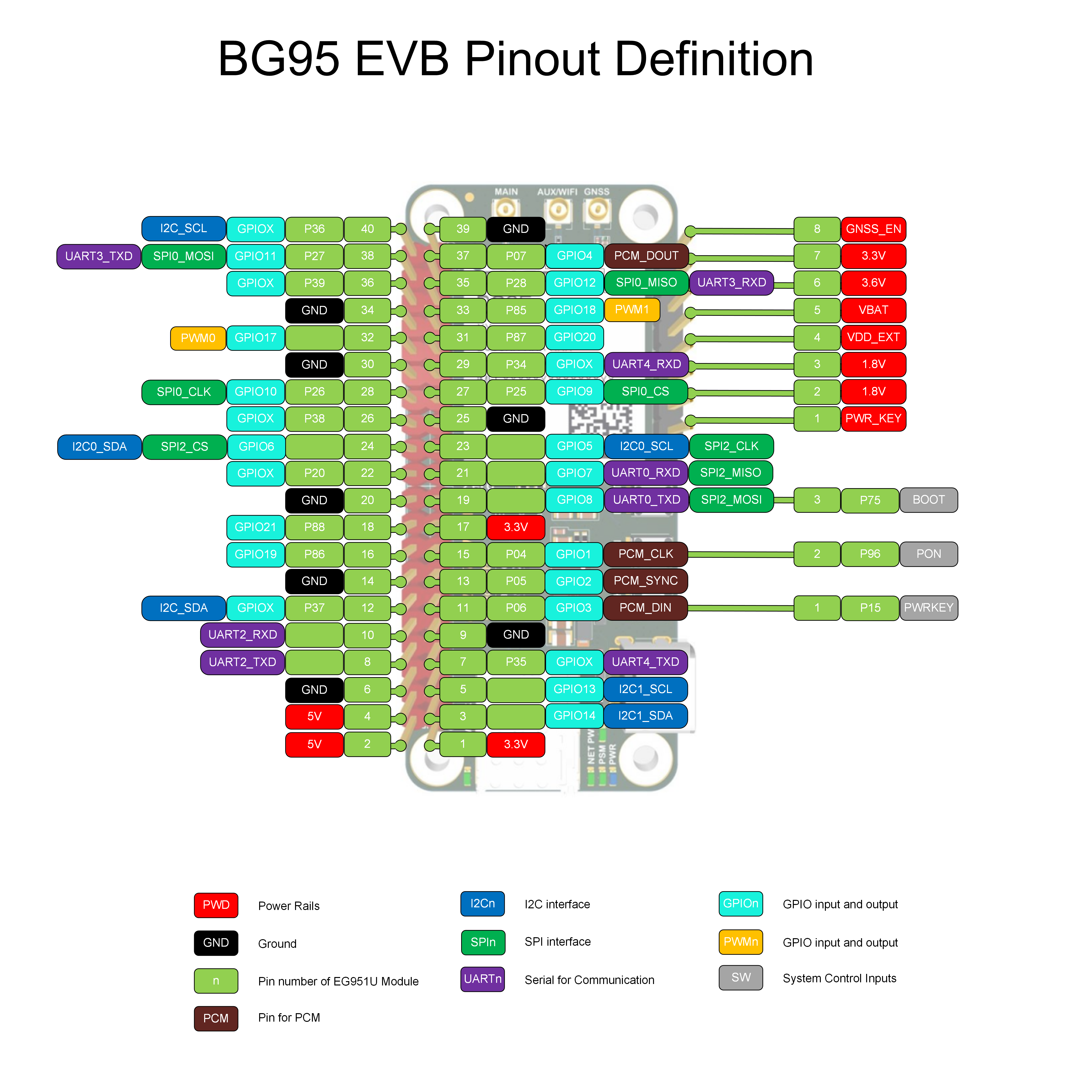
The main pin layout of the EVB is shown in the figure below.

Note
For more information about QuecPython_BG95_EVB, please visit https://python.quectel.com/en/resource-download?cid=5&pid=238.
EVB Configuration
The peripheral pin assignments are detailed as follows.
| No. | Name | Model | Supported | Silkscreen | Remarks |
|---|---|---|---|---|---|
| 1 | USB_TYPEC Interface | - | Yes | - | - |
| 2 | SIM Card Slot | SMN-315-ARP7 | Yes | CARD2 | Nano-SIM |
| 3 | LED Indicator (see below) | - | Yes | - | - |
On-board LED indicators:
- SIM_CHK: The SIM_CHK indicator lights up when a SIM card is inserted into the card slot.
- NET: Network indicator.
- PSM: Sleep mode indicator.
- PWM: PWM function indicator.
- PWR: Power indicator.
Refer to the silkscreen below the module in the EVB front figure (The module side) above for LED indicator locations.
Getting Started
First, you need a computer running Windows 10 or above.
- Step 1: Connect EVB
Connect the EVB Type-C port to your PC USB port with a USB Type-C cable for power supply.
- Step 2: Power on EVB
Short the two PWK_AUTO pins with a jumper cap to power on the board and it will turn on automatically, or long press the PWK button after power-on. It is recommended that the time interval between power-on and pressing the PWK button should be at least 30 ms.
After performing the above operations, wait for the power indicator on the main board to light up (silkscreen as PWR. You can refer to LED indicators above).
If the PWR indicator is constantly on, the EVB is successfully turned on.
